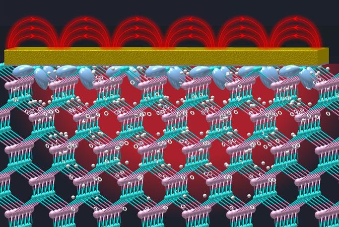
Researchers used a new light-bending technology to take advantage of semiconductor surface states and boost the wavelength conversion efficiency. Photo by Deniz Turan/UCLA
July 30 (UPI) -- Electrical engineers at UCLA have used a new light-bending technique to convert the wavelengths of light, a breakthrough that could boost the performance of many optical technologies.
Lightwave frequency conversion is key for a variety of imaging and sensing technologies, but the process is often inefficient, adding bulk and complexity to a variety of devices.
The new wavelength conversion technique -- described Friday in the journal Nature Communications -- relies on semiconductor surface states, a phenomenon that occurs when surface atoms aren't abundant enough to cohesively bind, yielding a breakdown in atomic structure.
Typically, electrical engineers try to avoid semiconductor surface states. Incomplete chemical bonds, also known as a "dangling bond," interfere with conductive abilities of semiconductors.
"There have been many efforts to suppress the effect of surface states in semiconductor devices without realizing they have unique electrochemical properties that could enable unprecedented device functionalities," Mona Jarrahi, professor of electrical and computer engineering at UCLA, said in a press release.
For the new study, researchers decided to take advantage of the large but shallow electric fields created by semiconductor surface states.
When struck by incoming light, electrons in a semiconductor lattice increase their energy state, allowing them to jump around within the lattice. The electric field further boosts the energy of the already excited electrons.
These hyperactive electrons unload their energy in the form of different optical wavelengths, thus completing the wavelength conversion.
Because the phenomenon is confined to the surface of a semiconductor, researchers deployed a nanoantenna array that bends light and traps photons within the semiconductor's surface layer.
"Through this new framework, wavelength conversion happens easily and without any extra added source of energy as the incoming light crosses the field," said lead author Deniz Turan, a postdoctoral researcher working under Jarrahi at UCLA Terahertz Electronics Laboratory.
Researchers successfully used their new technology to convert a 1,550-nanometer wavelength light beam into the terahertz lightwaves, featuring wavelengths of 100 micrometers up to 1 millimeter.
When scientists incorporated the light-bending technology into an endoscopy probe, which is used for in-vivo imaging and spectroscopy, they boosted the device's efficiency by a factor of 100.


